Register File, Part 1
add $r10, $r3, $r4 # R[10] = R[3] + R[4]The first step to executing this instruction is fetching the operands. In this case, we need to get the values of $r3 and $r4.
Recall that the CPU processes a 32-bit machine code instruction that's translated from the assembly code above, and encoded in that instruction are the 3 registers. In particular, each of the register is encoded using 5 bit UB.
For example, register 3 is encoded as 00011 and register 4 is encoded as 00100.
We're going to create a circuit called a register file. This circuit contains all 32 user-visible integer registers. We could create one for floating point, but that's not absolutely necessary. You'll still understand how a CPU works if we leave out floating point registers (they work pretty much like the integer registers).
We want the ability to access both registers (in this case, $r3 and $r4) at the same time. That way, we can save time. If we have to access one register at a time, it would slow down the execution of the instruction.
So, we have two sets of inputs to our register file, which specify which two registers we want. They can even be the same register.
Here's how our initial register file looks:
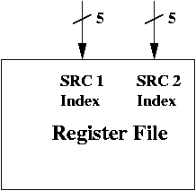
We've labelled the inputs as SRC 1 Index and SRC 2 Index, which are 5 bits each. We can think of registers 3 and 4 and source registers, and their result is stored in the destination register (in our example, it's $r10).
Register File, Part 2
Register File, Part 3
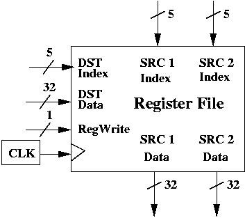
The DST Index comes from the instruction itself, just as SRC 1 Index and SRC 2 Index did. In our example, that's the encoding of $r10 (which is 01010).
It turns out we need one more input, in addition to DST Index and DST Data. Even though this particular instruction updates a destination register, not every instruction does so. We want to control when a register value is updated in the register file.
This control signal is called RegWrite and it's only 1 bit. If RegWrite = 1, then a write is performed on the register specified by DST Index, using the 32-bit data given by DST Data. If RegWrite = 0, then no write is performed. Both DST Index and DST Data are ignored.
Which reminds me, we have to talk about a clock. The register file also has a clock. The diagram below is now complete.
Why no RegRead?
You may wonder why there's no RegRead to control when the register file outputs SRC 1 Data and SRC 2 Data.The reason is simple. SRC 1 Data and SRC 2 Data are sent to the outside world (i.e., to other parts of the CPU). Those parts can simply choose to ignore the data, if they don't need it.
However, when you are performing a write on a register using DST Index and DST Data, you are updating the register file. The register file can't very well ignore that. To give it the option to ignore it, we must include RegWrite.
Clocks
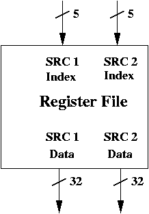
SRC 1 Data and SRC 2 Data are output with a small delay given a change in SRC 1 Index and SRC 2 Index. If you're curious about the implementation (or, more precisely, if you're curious about an implementation), look at the MAR from the previous set of notes.
You can see that it's hooked up to tri-state buffers. Once the tri-state buffers are enabled (which doesn't require a clock), the output is sent to the address bus.
Similarly, SRC 1 Index and SRC 2 Index enable two 32-bit tri-state buffers. In particular, they enable the tri-state buffers to the registers specified by SRC 1 Index and SRC 2 Index.
Again, this part does not need a clock. If SRC 1 Index and SRC 2 Index both change, then the tri-state buffers associated with the new registers are enabled (while the previous ones are disabled), and they are output after a small delay.
Writing Requires a Clock
However, when you want to write to a register, you are performing a parallel load on that register. This operation relies on a clock. We're going to assume that the register file, like MAR and MDR, is loaded on negative edges. This allows computations to be performed by the rest of the CPU before registers are loaded.Summary
Reading a value from the register file does not require a clock. Once you specify the registers you want to read (i.e., SRC 1 Index and SRC 2 Index), then there's only a small delay before the data comes out of the register file via SRC 1 Data and SRC 2 Data.
Writing a value to the register file does require a clock. You can specify which register you want to write to (using DST Index), the data you want to write (using DST Data) and whether you really want to write to the register file or not (using RegWrite). This action takes place on the negative edge of the clocks. (Positive edges are used to transition in the finite state machine and set up control signals for ALU, MUX, tri-state buffers, etc).