A Simple Model of a Computer
For example, a map models the roads in, say, a city. However, it doesn't tell you how much traffic is on each road, or where there are stop lights, or what offices or stores are near those roads. That information is either too difficult or too time-sensitive (i.e., it would get obsolete fast) to include in a map.
Our model of a computer is very simple, yet it has all the essential elements we need to understand these notes.
Here's an picture of our "computer".
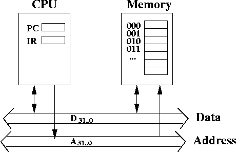
The CPU contains registers and an ALU. The memory contains data and instructions. The CPU is connected to the memory through two busses: a 32 bit data bus and a 32 bit address bus.
A Simple Model of Memory
When you first learned about arrays, you learned that an array has an index, and it has contents at that index. It's possible to confuse the two. After all, the index and the contents at that index are often numbers.
We don't use the word index to refer to an element at a location. Instead, we use the word address.
Memory is often said to be byte-addressable, which means that each address stores one byte. We could also talk about nybble-addressable (each address stores one nybble, which is 4 bits), or perhaps a word-addressable memory (each address stores one word, which we define to be 32 bits). However, it's very rare to see anything besides byte-addressable memory.
How to Store a Word
Most people would agree that you break the quantity into 4 bytes, and store them at four consecutive addresses in memory.
In particular, suppose you had a 32-bit word denoted as B31..0. You can divide this into four bytes: B31..24, B23..16, B15..8, and B7..0. We'll call B31..24 the most significant byte, or the high byte. We'll call B7..9 the least significant byte, or the low byte.
Let's say we store these four bytes at addresses 1000, 1001, 1002, and 1003.
However, there are two (common) ways to store four consecutive bytes. You can store high byte at the smallest address, i.e,, store B31..24 at address 1000 (and store B23..16 at address 1001, B15..8 at address 1002, and B7..0 at address 1003). This is called big-endian, because the big end (the high byte) is stored first.
Or you can store low byte at the smallest address, i.e,, store B7..0 at address 1000 (and store B15..8 at address 1001, B23..16 at address 1002, and B31..24 at address 1003). This is called little-endian, because the little end (the low byte) is stored first.
Even though a word takes up four addresses, we usually refer only to the smallest address when indicating the location in memory. So you simply have to be aware that you may be storing more than one byte, and thus more than one address in memory is being used.
Endianness affects any quantity larger than a byte. So halfwords (two bytes) have endianness, as do doublewords (eight bytes).
Word Alignment
A word-aligned address is an address that is divisible by 4. Equivalently, you can say it's an addresss that is a multiple of 4, or an address whose low two bits A1..0 = 00. That is, it's low two bits are both 0. (See why that's the same as being divisible by 4).
Halfwords are half-word aligned. This means half-words must be stored at addresses divisible by 2. This is equivalent to saying the address of a half-word aligned quantity, when written in binary, must have its least significant bit set to 0. That is, A0 = 0.
Doublewords are double-word aligned. This means double-words must be stored at addresses divisible by 8. This is equivalent to saying the address of a double-word aligned quantity, when written in binary, must have its low 3 bits set to 0. That is, A2..0 = 000.
In general, if you have 2k bytes, it must be stored at address that is divisible by 2k and that bits Ak-1..0 = 0k-1.
Some CPUs do not have word alignment, but nearly all RISC CPUs do, so it's important to understand the concept.
What Does the Memory Hold?
What is memory used for? It is used to store information. In particular, it can store:
- data This can be integers, floating point numbers,
MPEGS, JPEGs, or any variety of data formats. It can be the internal
representation of objects, etc.
- instructions One of the surprising ideas in computers
is the idea that instructions can also be stored in memory. A long
time ago, people thought of computers with highly specific purposes
(for example, computing trajectories of missiles), and didn't think
of it as general purpose. By allowing instructions to be "soft", i.e.,
represented just like data, it can be manipulated like data too.
- garbage Not every address stores meaningful data. Some of it is merely 0's and 1's without meaning.
In general, certain sections of memory are reserved for data, while other sections are reserved for instructions. Nevertheless, there's no inherent information stored in the bytes that indicate it's an instruction vs. data.
This has lead people to say "Information = Bits + Context". That is, bits do not have any meaning, except in certain contexts. Thus, if the CPU "thinks" there is an instruction at a certain address, then it will treat the binary value at that address as an instruction, even if it's not a truly meaningful instruction (i.e., it could be a valid instruction, but not within a meaningful program).
Thus, the CPU distinguishes between data, instructions, and garbage by context, not by any special tagging of the bytes to indicate what is stored. This means, in general, if you could inspect the bytes in memory, it might be difficult to tell if those bytes are data or instructions, or even if you could tell it was data, it would be hard to tell what kind of data it is.
Load/Store: Operations with Memory
To load bytes means to copy some bytes from memory to a register located on the CPU. This is the same as reading from memory to the CPU.
To store bytes means to copy some bytes from a register in the CPU to a memory location specified by a memory address. This is the same as writing from the CPU to memory.
A More Detailed Model of Memory
In particular, we're going to describe the pins associated with a memory chip. Pins are used for inputs and outputs of a chip. Some pins are for inputs (receiving information from the outside world). Some are for outputs (providing information to the outside world). Some are bidirectional (they do both).
First, we know that the CPU needs to access memory for either load or store. To do this, it needs to provide an address. So, we're going to assume memory has 32 bits of input for an address, which we label as A31..0.
In reality, there are many memory chips that are parts of memory. A large amount of memory is built from many memory chips. However, as far as the CPU is concerned, it can pretend that there is one monolithic memory chip (because of the interface memory provides). We'll do the same as well. We'll pretend there is one large 4 gigabyte memory chip.
Secondly, we need to tell memory whether we intend to read or write to memory. In this case, read and write are from the perspective of the CPU. Thus, to read from memory, means to get data out of the memory (so it can be sent to the CPU). This can be seen as a write from the perspective of memory. To write to memory means to get data into memory. This can be seen as a read from the perspective of memory.
We use the pin R/\W which is read as "read, not write". When R/\W = 1, we perform a read. When R/\W = 0, we perform a write. Usually, when we write something like \P we mean that P is active when 0 is input (this is also called active low). This is in contrast to writing it as P which is active when P is 1 (this is also called active high).
However, we don't always want to read or write. Sometimes we wish to do neither. (If we had to choose, it's better to do a read, since this does not update memory. However, reading makes the data bus unusable by other devices).
Thus, we have another input pin called CE for chip enable. Sometimes this pin is called chip select.
Since we do not write \CE, we assume CE is active high. That is, memory is enabled when CE = 1.
If CE = 0, then memory is disabled, which means memory ignores R/\W and performs neither a read, nor a write.
Finally, we need pins for the data. We assume these pins are bidirectional. They serve as input, when a write operation is being performed by the CPU (input to the memory chip, that is). They serve as output, when a read operation is being performed. They're ignored when the chip enable is not active.
We'll call these pins D31..0.
There's one more output pin from memory called ACK, which is short for "acknowledgement". It's not obvious why you need to have such a pin. It's purpose is to be involved in a protocol between memory and CPU for reading from or writing to memory.
A Diagram of Memory
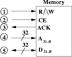
Legend of Pins
- R/\W (read/not write) This is a one bit input that comes
from the CPU. The CPU tells memory that it wants to perform a read by
setting R/\W = 1. It tells memory that it wants to perform a
write by setting R/\W = 0. However, memory only recognizes
this bit when CE = 1.
- CE (chip enable) When CE = 1, then the value of
R/\W is processed by memory (and a read/write is performced).
If CE = 0, memory neither reads nor writes. CE is
1 bit.
- ACK (acknowledgement) This is normally set to 0. When a
read or write is completed, ACK is set to 1. This wire is sent
to the CPU. It is reset back to 0 when CE is set to 0. ACK
is 1 bit.
- A31..0 (address bus). The CPU (or possibly
another I/O device) outputs the address to read or write.
- D31..0 (data bus). If the CPU is performing
a read (i.e., a load), then memory writes data onto the
data bus at the address specified by the address bus. The CPU
copies the data from the data bus to the CPU.
If the CPU is performing a write (i.e., a store) then it writes the data onto data bus. Memory copies the value into the memory location specified by the address on the address bus.
In both reads and writes, the CPU puts the address onto the address bus.
A Chart Describing Memory Operations
| CE | R/\W | Operation |
| 0 | 0 | No read nor write (since CE is not active) |
| 0 | 1 | No read nor write (since CE is not active) |
| 1 | 0 | Read data from memory (load) |
| 1 | 1 | Write data to memory (store) |
How It's Hooked Up
As you might guess, the address pins A31..0 are hooked up the address bus (see the diagram of the computer at the top of this page).
The data pins D31..0 are hooked up to the data bus (see the diagram of the computer at the top of this page).
What about R/\W and CE? These signals come directly from the CPU. So, the CPU isn't just hooked up to the data bus and the address bus. Assume there's a control bus where signals are sent between CPU and memory. There's three wires on this bus between CPU and memory: R/\W and CE go from CPU to memory. ACK goes from the memory to the CPU.
How Fast Is Memory?
Speed refers to the amount of time it takes to perform a read or write. Compared to performing those same operations on a register, reads and writes to memory are really, really, really slow. (Even slower still is accessing disk, which is incredibly slow).
Continuous Flow
For example, the CPU needs to keep asserting the value CE = 1 until a read or write operation is completed. It must also continue to assert R/\W as well. The CPU must also assert the address to the address bus until the operation is complete.
If the CPU is doing a write, then it must assert the data on the data bus, until memory sends back ACK = 1. If the CPU is doing a read, memory must assert the data onto the data bus until CE is set to 0.
The two biggest hurdles to understanding hardware is that values must be asserted onto a wire or bus until the operation is complete (it's not like making a function call, where you have a discrete computation). The second concept is that "everything" in hardware can be performed in parallel. Programming teaches us to think sequentially, but hardware is usually done in parallel.
Think of hardware like a city, where there are many businesses carrying out their activities in parallel. Occasionally, for some businesses (like building a house), you may need to wait for someone else to do their job before you can do yours.
Similarly, in hardware, there are many devices doing things in parallel. Of course, they are all working together to run assembly language instructions.
Summary
Think of this as an interface (just like a Java class interface). This is how the CPU views memory. The actual implementation may involve many memory chips hooked up in such a way to give the illusion that there is one monolithic chip. This goes to show you that hardware has abstractions, just as software does.
The amount of memory in the CPU is very limited (roughly 128 bytes, due to 32 32-bit registers), so most information is stored in memory. Memory stores data, instructions, and garbage.
While certain regions of memory are reserved for code and other regions for data, the CPU basically distinguishes between code and data by context. This means there is no "tagging" or "labelling" of bits in memory. Thus, if you could inspect the binary values in memory, you would (in general) be unable to tell what the binary values stood for. The CPU generally assumes certain addresses contain data and certain addresses contain code. If these assumptions are incorrect, errors occur.
The CPU accesses information from memory sending addresses and control signals to memory. It may either send or receive data depending on whether a read or write operation is being performed.
Accessing memory is very slow compared to accessing registers which reside directly on the CPU. Registers can be accessed in about 0.25 ns while memory can be accessed in about 100 ns. Thus memory is about 400 times as slow as registers. Despite the speed (or lack thereof) of memory, the CPU must access memory because the CPU has very little memory of its own.