Baby Steps
MAR
MAR is short for memory address register. This register has its output hooked up to the address bus. This register is going to be the only way for the CPU to communicate with the bus.However, to prevent the memory address register from continously dumping its output to the address bus, we'll place a 32-bit tri-state buffer between the output of the MAR and the address bus. This allows other devices (say, I/O devices) to use the address bus, if necessary.
The MAR can hold two different kinds of addresses. Either it stores the address of an instruction, or it stores the address of data. Of course, as far as memory is concerned, an address is an address. It doesn't care what is stored at that address.
However, from your perspective, as a person learning how a CPU works, it's useful to know that MAR can hold either an instruction address or a data address.
Where does the MAR load its addresses? For now, we're just going to say that it comes from some other part of the CPU, which we'll discuss at a later point.
MDR
MDR is short for memory data register. As you might guess, the MDR is the analog of the MAR, except it is used with the data bus, instead of the address bus. Unlike the MAR, where we either place the address on the address bus or we don't (by deactivating the tri-state buffer between the MAR and the address bus), the MDR has more operations than just placing the data on the data bus or not placing it.In particular, data can go both ways. For a load operation, we expect to read data from the data bus into the MDR. For a store operation, we expect to place the data from the MDR onto the data bus.
This means that the MDR can (parallel) load its data from one of two places: the data bus (for a load operation) and somewhere else in the CPU (for a store operation).
We want to provide two choices for where the MDR should get its data. What kind of circuit should we use that allows us to select from one of two different inputs? A 2-1 MUX! Specifically, a 32-bit 2-1 MUX.
Similarly, the data from the MDR can either go to the data bus (for a store operation) or to some other part of the the CPU (for a load operation). Although it looks like we may need a DeMUX, we won't. We'll just split the data up, and both places will get the data.
A Diagram
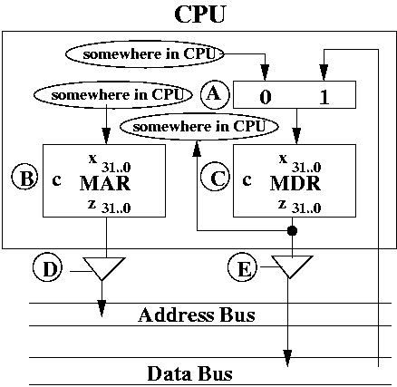
So far, the CPU contains two registers. MAR is on the left. MDR is on the right. The input to the MAR comes from some other place in the CPU, which we'll discuss later on.
The output of the MAR is hooked to the address bus using a 32-bit tri-state buffer.
The inputs to the MDR comes from one of two places. Either it comes from some other place in the CPU (for store operations) or it comes from the data bus (for load operations). A MUX is used to pick which input the MDR should load from.
The output of the MDR is hooked to the data bus using a 32-bit tri-state buffer. It is also directed to some other place in the CPU, which presumably uses the data in the MDR after it has been loaded from the data bus.
The diagram may seem confusing, but you should look it over until you feel comfortable with what's going on.
I've left of the drawing of memory, which would be hooked up to the address and data bus, as shown from a previous set of notes (see the initial Roadmap notes). However, you should assume that memory is still there.
Control Signals
Let's list them out.
- A This is the control to the 32-bit 2-1 MUX to the MDR.
Either the MDR can get its input from the data bus or from some other
part of the CPU to be specified later on.
- B This is the control to the MAR. You can either
load or hold.
- C This is the control to the MDR. You can either
load or hold.
- D This is the control to the tri-state buffer
from the MAR to the address bus. The control can either be on
(allowing the bits to flow through) or off (allowing nothing to
flow through).
- E This is the control to the tri-state buffer from the MDR to the data bus. The control can either be on (allowing the bits to flow through) or off (allowing nothing to flow through).
The control signals are going to become very important soon because they will allow use to control when the CPU does what. In particular, we're eventually going to talk about the design of a control unit, which will orchestrate the events in a CPU.
We're going to classify control signals into two types:
- Operations on registers (i.e., parallel load and hold)
- Operations on combinational logic devices (e.g.,. MUXes, tri-state buffers)
The biggest difference between these two kinds of signals is that one is based on a clock (i.e., sequential devices such as registers) and the other one is not (i.e., combinational logic devices).
Even though the second one is not based on a clock, the entire CPU runs using a clock, and so, indirectly, the clock is important when it comes to dealing with combinational logic devices.
We'll discuss these issues in a future set of notes.
Hidden Registers
Think of them like local variables to a function. For example, you may have been assigned to write a function that takes two parameters and returns some value. To compute the return value, you may need to declare some local variables. Whoever uses the function does not have to be aware of the local variables, and that they are used to help with the function.
Similarly, users do not need to be aware of the MAR and the MDR. Over time, we may decide it's not necessary to have the MAR or the MDR. Because they are hidden, it shouldn't affect the running of the assembly language programs, since they don't use these registers.
Summary
We use tri-state buffers and a MUX to control where the data comes from and where the data goes to with these two registers.
Later on, we'll fill in those details, as we extend our implementation of the CPU.