However, 232 is 4 gigabytes, which is extremely large, especially for the time. This brings about a very interesting point. Even though CPUs have enough address pins to address large amounts of memory, it's not always the case that there is any RAM at all memory locations!
You can create combinational logic circuits that determine whether an address is valid or not, and send a signal back to the CPU if the address is invalid. This is left for another set of class notes (which currently don't exist).
To create the memory you needed, you put together one or more chips of RAM.
Let's assume, for simplicity's sake that our computer can only access 4K of RAM. The amount memory is quite small even twenty years ago, but makes it easy to illustrate the point of interleaved memory.
However, we have chips that contain only 1K of RAM, thus we need four such chips to create a total of 4K.
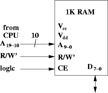
Let's look at the various pins of this chip.
Where do the signals to the RAM come from? The address bits come from the CPU. The CPU has 32 bits of address, A31-0. Clearly only 10 bits can go to this chip since the chip only has 10 address bits.
Does it have to be bits A9-0? Not necessarily. Any 10 bits will do. In the diagram above we see A19-10 fed from the CPU (via the address bus) to the RAM. It may not make any sense to wire the RAM in this way, but it is possible to do so.
R/W' is one of the control signals the CPU can send to RAM>
We'll need to develop the logic for the chip enable in a moment.
We can think of a software analogy. Suppose you want to allow a person using your program to access 4096 array elements. However, due to a strange programming language, arrays only have a maximum size of 1024 values.
How might you give the illusion that you have 4096 values? One way to do so is to declare four arrays of size 1024. Call these arrays arr0, arr1, arr2, and arr3. The user thinks they have an array called arr with indexes from 0 up to 4095.
In reality, when the user wants to access index 0 through 1023, you get the value from arr0. If they want to access values from index 1024 to 2047, then you subtract 1024 from the index, and access the array element at the new index from arr1.
If they want to access array elements at index 2048 to 3071, then you subtract 2048 from the index, and access the array element at the new index from arr2. You can do similar things for arr3.
Thus, you can create the illusion you have a much larger array even if the language imposes restrictions.
Here's one way we can map memory to the chips.
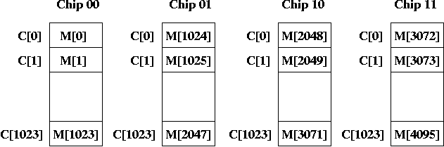
Each chip is indexed by 10 bits which are the address bits. The index goes from 0ten up to 1023ten.
I've also numbered the chips (in binary) as chips 00, 01, 10, and 11.
Suppose someone asks you where M[1025] stored. Your answer would be in Chip 01 at index 0. If someone wanted to know where M[3071] is stored, you would say it's in Chip 10, at index 1023. M[1023] is like a virtual element, and the actual element is in Chip 01 at index 1023.
Suppose the amount of time to access one byte from a RAM chip is T. Then, it will take 4T to access 4 consecutive bytes at a word aligned address. That's because 4 consecutive bytes all reside on the same chip, and it takes time T to get each byte.
If we didn't care about getting word-aligned words, we might be able to do better, but we'd have to be very lucky. If you want M[1022], M[1023], M[1024], and M[1025], you can access this in 2T time.
That's because the first two bytes are in Chip 00 and the last two bytes are in Chip 01. So you can access one byte at a time for both chips in parallel. However, there's only a small number of addresses that work like this.
Can we do better? Can we access four bytes of memory in T time instead of 4T?
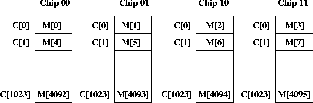
Thus M[0] is on Chip 00, M[1] is on Chip 01, M[2] is on Chip 10, M[3] is on Chip 11, and M[4] is back on Chip 00.
Notice that if we access a word aligned quantity, the first byte always appears on Chip 00. Furthermore, because we access four consecutive bytes, they are always at the same index on every chip.
For example, if we want a word starting at address M[4092], we access index 1023 of all four chips. This allows us to access words in T time.
In the example above, we have four way interleaving, since a chip contains every fourth byte.
If someone asks where is M[5], you can say it's on Chip 01 at index 1. If someone wants M[2], it's at Chip 10 at index 0.
In general, where is M[i]?
For example, if you want M[103], then this is at chip 103 % 4 = 3 (i.e., Chip 10), and the index is at 103 / 4 = 25 (using integer division).
Equivalently, think of the address in binary. The chip is the low two bits. The index is bits B11-2.
Let's think about what chips are enabled under various circumstances.
What do you notice about the memory addresses in Chip 01? They are M[1], M[5], M[9], etc. All those addresses are congruent to 1 mod 4 (that is, dividing the index by 4 leaves a remainder of 1). Equivalently, the low two bits of the binary address are 01. This is why it's called Chip 01.
What do you notice about the memory addresses in Chip 10? They are M[2], M[6], M[10], etc. All those addresses are congruent to 2 mod 4 (that is, dividing the index by 4 leaves a remainder of 2). Equivalently, the low two bits of the binary address are 10. This is why it's called Chip 10.
Finally, what do you notice about the memory addresses in Chip 11? They are M[3], M[7], M[10], etc. All those addresses are congruent to 3 mod 4 (that is, dividing the index by 4 leaves a remainder of 3). Equivalently, the low two bits of the binary address are 11. This is why it's called Chip 11.
From this observation, you see only the addresses in Chip 00 are word-aligned, i.e., only Chip 00 can contain the first byte of a word. Also, Chips 00 and 10 are halfword aligned, so only those chips can contain the first byte of a halfword.
Putting all these facts together, we generate the following Boolean
expression for chip enable for Chip 00.
CE = W + (H * A1') + (B * A1'A0')
The circuit looks like this:
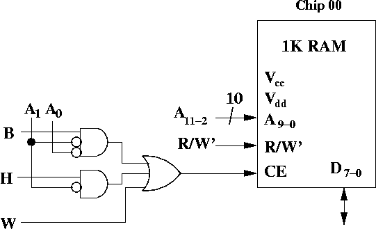
In particular, pay attention to the input to A9-0. Remember that when we wanted to get M[i], we accessed index i / 4. This is the same as shifting the bits right by 2, or equivalently, accessing bits A11-2 from the address bus.
Thus, A11-2 comes from the address bus, while R/W' is a control signal from the CPU.
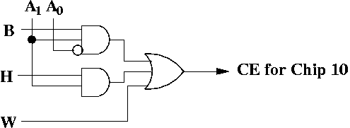
Here's the logic for the chip enable for Chip 10.
CE = W + (H * A1) + (B * A1A0')
This is how the chip enable logic looks for Chip 10.
To convince yourself it works, try writing the logic for all four chips, then pick some address like 10, and see what happens if, say, H = 1. See which chips are enabled. Make sure if H = 1 you pick a halfword aligned address, and if W = 1 you pick a word aligned address.
One possibility is to make sure those 20 bits are 0 (using a very large NOR gate), and using the output of the NOR gate, then AND that result with the chip enable from above, and feed the result of that into the chip enable.
Otherwise, you are essentially allowing any address that has the correct low 12 bits to access the chips, and the upper 20 bits become irrelevant. If this isn't a problem, you don't have to deal with it, but you can assume that if the upper 20 bits are not all zeroes, then none of the chips are enabled.
Admittedly, the CPU must still sort out the bytes it does get, but we assume it can do that.