A Simple Model of Memory
Introduction
A basic computer consists of a CPU, which processes instructions,
memory, which stores data and instructions, and a bus, that connects
the CPU to memory.
We're going to focus on memory in these notes. Initially, we'll
have a very simple model of memory, then we'll make it a little more
realistic.
Memory as a Large Array
It's useful to think of memory as a large array. Since you've
been programming for several semesters now, arrays are something you
should be experts with.
Think of memory as a large one-dimensional array.
But arrays have types! So what type of array should memory have?
Each element of memory contains a byte. Let's now define
two terms
Definition An address is another name for the index of
an array. It's often called address rather than index, when used
with memory.
Definition Byte-addressable memory means that at each
address, there is a byte. That is, memory consists of an array
of bytes.
We could have nybble-addressable memory (each address stores
a nybble) or bit-addressable memory (each address stores a bit)
or word-addressable memory (each address stores a word).
However, the most common use of memory is to have one byte at each
address.
Multiple-byte quantities
How do you store multiple byte quantities in memory? For example,
suppose you want to store 32 bits. One way to store this is to break
the 32 bits up into 4 bytes, then store the 4 byte quantity in
consecutive order. For example, if the first byte is stored at 1000,
then the next 3 bytes are stored at 1001, 1002, and 1003.
Endianness
As it turns out, storing multiple bytes is a little more complicated
than that. For example, when you break a quantity into 4 bytes, and
store it in memory, there's two popular ways to do this. One way
stores the least significant byte of a four byte quantity in the
smallest address first (at address 1000, in this example), and works
its way to the most significant byte (at address 1003). This is
called little-endian ordering.
If you store the most signficant byte first (at address 1000),
and work your way to the least significant byte (at address 1003),
that's big-endian ordering.
To make things more complicated, this ordering is only performed
on quantities that the CPU handles. If you're storing a structure,
for example, a structure can be broken down into bytes, halfwords,
and words. The entire structure usually does not have
an endianness, but its individual components do. For example, if
a structure contains an array of int, then each element has
an endianness, but if you look at the array's elements, they always
increase in addresses. Thus, & arr[ i ] is less than
& arr[ i + 1 ].
Word-alignment
To make things even more complicated, word quantities are
often word-aligned (first byte stored at an address divisible by
4), while half-words are half-word aligned (first byte stored
at an address divisible by 2), and double-words are double-word
aligned (first byte stored at an address divisible by 8).
How does a computer know about words? It turns out that there are
instructions to read and write from memory, and those instructions
often specify a size. For example, if the instruction is to load
a word, then the word must be at a word-aligned address. If it
loads a byte, then it can be at any address. We'll explain
what it means to load a word momentarily.
"Dumb" Memory
As it goes, it's the CPU that is aware of endianness and aware
of word alignment. Memory is "dumb". It merely access the bytes
it's being asked to retrieve or to write to. It does not place
meaning to the bytes, like the CPU does.
Basic Memory Operations
The CPU performs two kinds of operations on memory. It can
either read from memory (this is called a load), or it
can write to memory (this is called a store).
Read
When reading from memory, the CPU
- specifies an address in memory,
- plus the number of consecutive bytes it wants (usually
1, 2, 4, 8 bytes are the only possibilities), starting at the
address specified,
- plus the fact that it wants to read from memory
How does it do this? The address is sent to memory via the
address bus. The number of bytes can be sent in a signal through
the control bus. Also, the fact that the computer wants to do
a "read" operation can be sent through the control bus.
Once memory has received the signals, it retrieves the data from
memory, and outputs the data to the data bus, and alerts the CPU that
the quantity is now available, at which point the CPU will then read
the data off the data bus, and store the information internally in a
register.
Write
For a write operation, the CPU
- specifies an address in memory,
- plus the number of consecutive bytes it wants to store (usually
1, 2, 4, 8 bytes are the only possibilities), starting at the address
specified,
- plus the fact that it wants to write from memory
- plus the data it wants to write to memory
How does it do this? The address is sent to memory via the
address bus. The number of bytes can be sent in a signal through
the control bus. The CPU also informs memory it wants to do
a "write" operation through the control bus. Finally,
it places the data from the CPU onto the data bus (usually from
a register).
Once memory has received the signals, it reads the data off the
data bus, and then stores the data at the address specified.
Pin Specifications
Once we know the operations, we can begin to specify what "pins"
the memory contains. Pins refer to inputs or outputs of the memory.
If you've ever seen any hardware (say, a CPU or memory), you will
sometimes see pins. CPUs especially have lots of pins. Some of
those are inputs, some are outputs, some are both input and output.
These are the various pins memory should have, assuming 32 bit
addresses and word sizes of 32 bits.
- A31-0 32 pins for the address bus.
- D31-0 32 pins for the data bus.
- R/W' A one bit quantity that indicates whether a read or
write operation is requested of memory. When R/W' = 1, a
read is requested by the CPU to memory. When R/W' = 0, a
write is requested by the CPU to memory.
- CE' A one bit quantity called chip enable.
If CE' = 0, then the CPU wishes to do either a read or
write operation on memory. The exact operation is specified
by R/W'. If CE' = 1, then the CPU does not
want to do either a read, nor a write operation. After all,
the CPU may not always want to perform an operation on memory.
We write CE' (CE with a prime after it) to indicate that
this is an active-low signal. An active-low signal
means that the signal is "active" when the value is 0. Thus,
chip-enable is enabled when the signal is 0. If it were active-high,
we would leave the prime off (write it simple as CE), and
then 1 would make CE active, instead of 0.
- ACK This is a 1-bit output pin that stands for
"acknowledgement", that informs the CPU that either the read or
write operation has been successful. When the value of
ACK goes to 1, the CPU knows the memory has completed the
operation. The CPU responds by setting CE' to inactive
(i.e., it sets the value to 1).
- Vcc, Vdd. These pins are
for power, and have nothing to do with data, address, or control.
The chips require power to run, and these provide the voltages
and currents to make it run.
Diagram of Memory
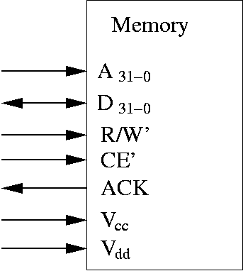 Some comments:
- The address pins are input only (i.e., A31-0).
There are 32 pins. This is connected to the address bus.
- The data pins are bidirectional (i.e., D31-0).
They can be used to place data into memory or copy data out of memory.
There are 32 pins. This is connected to the data bus.
- One input pin for R/W'. This is connected to the control bus.
- One input pin for CE'. This is connected to the control bus.
- One output pin for ACK. This is connected to the control bus.
- One input pin for Vcc and Vdd.
This is hooked to power and ground.
Why it's Simplified
We've left a few details out. First, we said there's a way to
specify the number of bytes to be retrieved. The memory chip shown
above does not have such pins. They could be easily added. For now,
you can assume that it retrieves 32 bits at a time.
In reality, it's probably easier to fetch 8 bytes or more, and then
pick out the bytes you actually need. The data bus actually controls
how much data you can get at a time.
Also, we assume this chip contains 232 bytes (which
is 4 Gigs). In reality, you usually have far less memory than this.
Usually, you only have maybe 1 G of physical memory. In the past,
even 64 M of memory was quite a lot.
Also, the memory system is often built from many smaller memory
chips, and logic that connects them all. Furthermore, if you do
memory-mapped I/O, not all addresses are devoted to real memory.
Some are devoted to I/O devices.
These details are lead to additional complication, even if it's
more realistic.
Web Accessibility