Read-only memories allow you to read, but not modify the memory. The idea is to initialize the memory once, and then use it as a kind of lookup table from that point onward. ROMs can be used as a kind of control unit, but we'll not discuss that right now.
Some ROMs are programmable multiple times. For example, an EPROM is short for an erasable programmable read-only memory. You can erase the contents of the EPROM, typically, by exposing it to ultraviolet light, then "burning" the new contents in. EEPROM are short for electrically erasable programmable read-only memory. Electrical currents can be used to erase the contents (making it easier to reprogram).
RAM (random access memory) often needs a refresh current to keep the contents of memory active, while ROM can often retain the contents even when power is removed.
Think of ROMs as an extension to the MUX trick.
| Row | x | y | cin | cout | s |
| 0 | 0 | 0 | 0 | 0 | 0 |
| 1 | 0 | 0 | 1 | 0 | 1 |
| 2 | 0 | 1 | 0 | 0 | 1 |
| 3 | 0 | 1 | 1 | 1 | 0 |
| 4 | 1 | 0 | 0 | 0 | 1 |
| 5 | 1 | 0 | 1 | 1 | 0 |
| 6 | 1 | 1 | 0 | 1 | 0 |
| 7 | 1 | 1 | 1 | 1 | 1 |
Let's implement both cout and sum.
To do so, we use an 8-1 2-bit ROM. Each address of ROM contains a 2-bit quantity. Unlike the MUX, the bits are stored inside the ROM itself. Thus, a ROM is not a combinational logic circuit, since combinational logic circuits do not have memory.
In general, memory circuits are slower than combinational logic circuits.
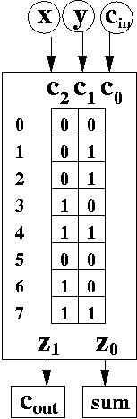
Let's look at the ROM above. The ROM has 3 address bits c2c1c0 which we still call control bits. This allows us to pick one of 8 possible addresses. Each address (for this ROM) stores 2 bits. We can imagine ROMs storing any number of bits at each address, not just 2 bits, as shown above.
Suppose c2c1c0 = 100. This selects address 4. In the example above, address 4 contains the two bit quantity 11. This quantity is then output as z1 z0 at the bottom of the ROM.
We can use ROMs very much like we use MUXes. They can be used to implement truth tables. There are differences between the two. The MUX use hardwired 0's and 1's which come from outside the MUX, and are fed into the inputs. By contrast, the ROM stores the information inside the ROM itself. Thus, you see 16 bits of memory in the ROM (8 addresses, with 2 bits per address).
Let's see how this ROM implements the full adder, whose truth table was given above.. Look at the address bits c2c1c0 = 001. In the ROM example shown above, that address contains bits 01. Why did we put 01 at that address?
01 also corresponds to the two bits of row 1 in the full adder truth table above. If you look at that row, cout = 0 and sum = 1. Thus, for each row of the truth table, we copy the outputs bits to the corresponding address in the ROM. Thus, the output bits row 0 are copied to the bits of address 0. The output bits of row 1 from the truth table are copied to the bits of the ROM at address 1, and so on for all 8 addresses.
It's easy to make a ROM output a truth table with multiple outputs.
The point of the trick is to allow you to implement circuits quickly in exam situations.