When you think combinational logic, you should think "once the input arrives, the combinational logic starts processing it to make outputs".
When you think sequential logic, you should think "once the input arrives, you have to wait until the next positive clock edge, before the input can be read in and processed".
These two views help you reason about computer systems.
We're at the stage of the course where we want to put the pieces of the CPU together, and we're interested in seeing how a CPU gets built, and how it works. In my opinion, this is the central part of computer organization.
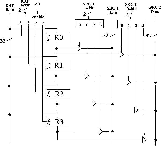
In particular, we begin by understanding how to put together a register file. A register file is essentially a black box, and a black box is the hardware equivalent of a function.
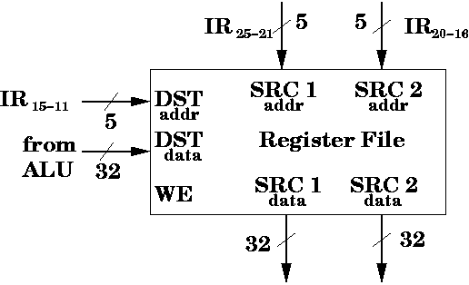
Here's a diagram of a register file.
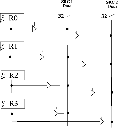
A MIPS CPU has 32 integer registers within the register file. However, we only need four registers to demonstrate how to implement a register file.
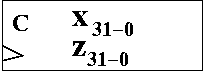
It has a 32 bit input, x31-0, a 32 bit output z31-0, one control bit, c, and a clock input. When c = 1, the register parallel loads, i.e., z31-0 = x31-0. When c = 0, it holds the value.
We attach the outputs of each register to two busses, using two tri-state buffers.
Here's a diagram.
How do we tell the register file which registers we want? Through the SRC 1 addr and the SRC 2 addr. Since our register file only contains 4 registers, we only need 2 address bits to specify which tri-state buffer to make active. Notice that, we specify one register per bus.
We need to hook this combinational logic circuit to four tri-state buffers. Thus, we have two bits of input, which specify the register, and four outputs to hook up to the tri-state buffer. And since we only want one of the tri-state buffers to be active, then only one of those outputs should be a 1, while the rest are 0.
There's only one combinational logic device (OK, there's actually two) that meet this requirement: a 2-4 decoder.
A 2-4 decoder takes two bits of input, interpreted as a 2-bit UB number, and makes exactly one output 1, while the rest of the output are 0.
Let's add the two decoders.
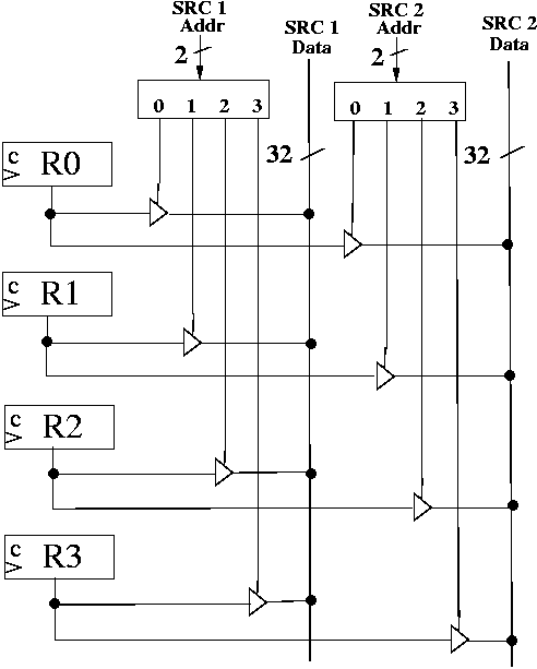
We've taken care of SRC 1 Addr and SRC 2 Addr (using 2 bits, instead of 5, since we have 4 registers in this implementation, instead of 32 registers). We've also incorporated SRC 1 Data and SRC 2 Data. These are 32 bits busses.
We're missing, DST Addr and DST Data. We also need Write Enable. What is write enable used for?
Suppose we have an instruction like add $r1, $r2, $r3. Then, $r1 is the destination register. We can specify it using two bits: 01. The DST data is the data to be written to the destination register, at the next positive clock edge.
However, we don't always want to write to the register file at every positive clock edge (for example, in a branch or jump instruction, no register is updated). We need someway of indicating to the register file when we want to write, and when we don't.
That's what Write Enable (or WE for short) is used for. When WE = 1, we write to the register, specified by DST Addr. When WE = 1, we don't do anything. We want all registers to maintain or hold their values.
How can we implement this? We have two bits of inputs from DST Addr. We want want only one of the registers to parallel load, and only if WE = 1. Thus, only one parallel load register should have value c = 1, while the rest have 0, and that's only if WE = 1.
What combinational logic device can we use? There are two choices, which are basically the same. Either use a 2-4 decoder with active-high enable or use a 1-4 DeMUX. We'll use the first.
You've seen how to construct all of these devices, so you know where they all come from!